

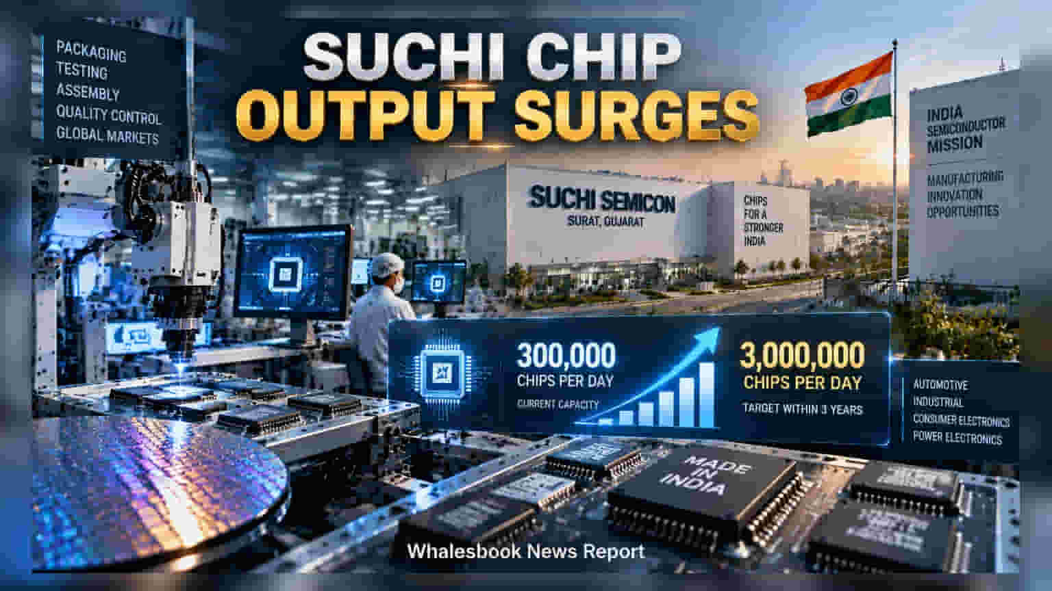
Suchi Semicon has launched commercial operations at its Surat facility, with an initial output of 300,000 chips per day. The company plans to scale this capacity to 3 million chips daily over three years. Supported by the India Semiconductor Mission, the project targets the automotive and industrial sectors, making it a key step in India’s efforts to build a domestic chip packaging ecosystem.
Suchi Semicon has officially commenced commercial production at its semiconductor packaging and testing facility located in Surat, Gujarat. The plant is one of the first Outsourced Semiconductor Assembly and Test (OSAT) units approved under the India Semiconductor Mission to move from initial project approval to the operational stage.
Scaling Production and Capacity Targets
The facility currently operates with a capacity to package and test approximately 300,000 chips per day. The company has outlined an ambitious growth plan to increase this output tenfold, targeting 3 million chips per day within the next three years. This scale-up is intended to support a wide range of applications, including automotive, industrial, consumer electronics, and power electronics. To achieve this, the company plans to integrate advanced packaging technologies such as SOIC and QFN at the Surat site.
Investment and Market Context
The project involves a total investment of US$100 million and received government support of ₹868 crore under the national semiconductor incentive programme. The collaboration with Japan's ROHM Semiconductor for technology transfer is a key component of the company’s strategy to meet the quality standards required by global firms.
For the Indian semiconductor market, this transition from construction to commercial output is a critical development. OSAT facilities are essential to the broader supply chain, as they handle the final stage of chip manufacturing—packaging, testing, and verifying the functionality of semiconductor devices before they are sent to end-users.
Operational Risks and Future Monitorables
While the start of commercial production is a positive milestone, investors and stakeholders should note that the semiconductor business carries specific execution risks. The success of the facility will depend on the speed of customer qualification. In the semiconductor industry, it typically takes between six months and one year for new packaging facilities to get their processes and quality certified by global chip companies.
Revenue generation is directly linked to these qualifications. If global semiconductor firms do not approve the facility’s output within expected timelines, the ramp-up to 3 million chips per day could face delays. Furthermore, as the company scales, managing high capital spending and ensuring the facility achieves high capacity utilisation will be vital to maintaining profit margins.
Looking ahead, market participants will likely monitor the company’s ability to secure new global clients and the timelines for its planned expansion into more advanced packaging segments. The company has stated that current customer demand supports its expansion plans, but the actual pace of scaling will be the most significant factor in its long-term financial performance.