

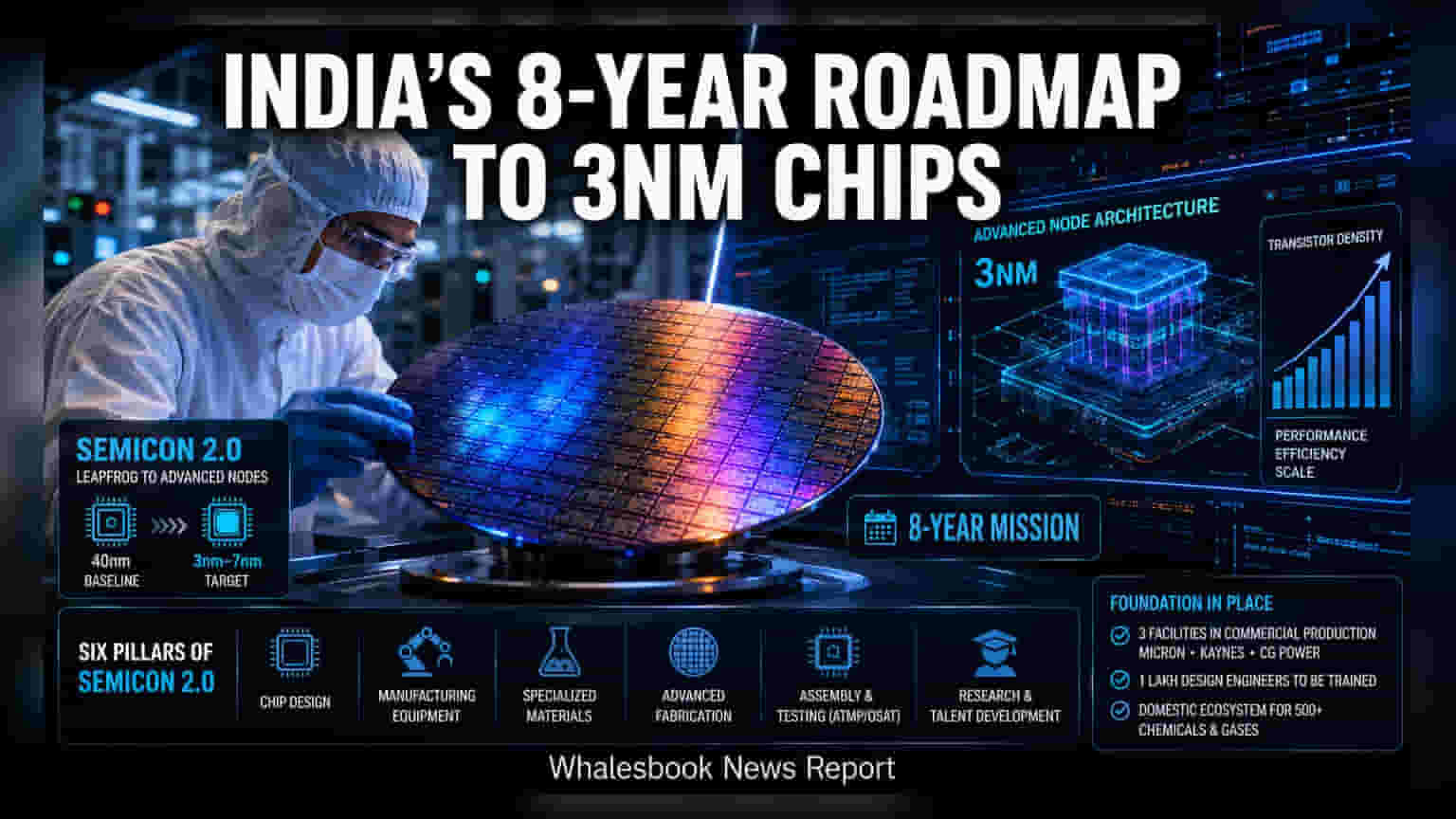
India has launched the 'Semicon 2.0' mission with an ambitious goal to achieve domestic production of advanced 3nm-7nm chips within eight years. The strategy moves beyond simple assembly to build a full supply chain, including equipment and specialized materials. While this marks a significant jump in technological ambition, investors should note the high capital intensity and the operational challenges involved in mastering such complex fabrication processes.
The Indian government has officially rolled out the second phase of its semiconductor mission, known as 'Semicon 2.0,' marking a strategic pivot toward high-performance chip manufacturing. While the initial phase focused on establishing foundational fabrication and packaging units, the new roadmap sets a target of achieving domestic production for 3-nanometre to 7-nanometre chips within the next eight years. This is a significant leap in complexity from the 40-nanometre baseline currently utilized in early domestic projects.
A Six-Pillar Strategy
The government’s approach under Semicon 2.0 is designed to build a self-reliant ecosystem rather than relying solely on imported technology. The policy is structured around six key pillars: chip design, manufacturing equipment, specialized materials, advanced fabrication, assembly and testing (ATMP/OSAT), and research and talent development. By incentivizing the domestic production of the 500+ specialized chemicals and gases required for modern chipmaking, the government aims to insulate the local sector from global supply chain disruptions.
As of August 2026, the foundational work is already underway. Three facilities, spearheaded by companies including Micron, Kaynes, and CG Power, have reached the commercial production stage. These units are critical as they provide the operational base upon which the more advanced fabrication technologies will be layered in the coming years. The government has also emphasized human capital, with plans to train one lakh design engineers to support the industry’s long-term growth.
Investor Considerations and Risks
For investors, the move into 3nm chip production represents a high-stakes transition. Establishing fabrication units at this scale is extremely capital intensive, with costs for a single facility capable of advanced node manufacturing estimated to reach $15 billion. The financial viability of these projects depends heavily on consistent demand and the ability of companies to manage high operational costs.
Beyond capital spending, the primary risk remains execution complexity. Moving toward 3nm and 2nm nodes requires precise yield management, where minor defects can lead to significant production losses. Furthermore, these high-end manufacturing processes are highly dependent on reliable, high-quality infrastructure, including stable power grids, large volumes of ultra-pure water, and a steady supply of specialized industrial inputs.
Investors may monitor the progress of private investment inflows and the actual implementation of these six pillars. The long-term success of this roadmap will likely depend on whether the domestic ecosystem can achieve the efficiency needed to compete with established global manufacturing hubs, while managing the cyclical nature of semiconductor demand.