

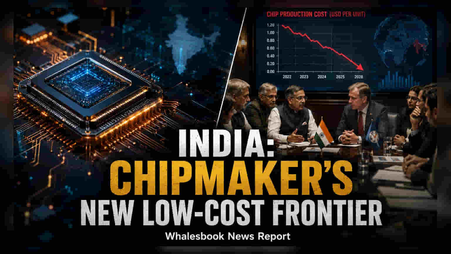
The government has approved the second phase of the India Semiconductor Mission with a ₹1.27 lakh crore outlay. This initiative aims to attract chipmakers by offering over 10% in cost savings through incentives and lower operational expenses. Investors may watch how this push impacts the domestic electronics supply chain and long-term capital allocation for participating firms.
The Indian government has officially greenlit the second phase of the India Semiconductor Mission (ISM 2.0), committing a substantial ₹1.27 lakh crore to accelerate domestic chip manufacturing. This expanded strategy moves beyond the initial focus on fabrication and packaging, aiming to build an end-to-end ecosystem that includes semiconductor design, specialized materials, and manufacturing equipment. The government also plans to notify a separate ₹62,500 crore mobile manufacturing scheme within the next twenty days to further strengthen the domestic electronics production landscape.
Strategic Cost Advantages and Incentives
To attract global and domestic players, the India Semiconductor Mission is highlighting a potential cost advantage of over 10% compared to existing global manufacturing hubs. According to Amitesh Kumar Sinha, CEO of the mission, this competitiveness is driven by a combination of state and central government incentives and lower local operational costs. Government support is designed to cover a significant portion of capital spending through depreciation-linked incentives. By providing these subsidies, the government intends to help new Indian facilities achieve a cost structure similar to older, fully depreciated plants in other countries, which is a major hurdle for new entrants in the semiconductor industry.
Operational Efficiencies and Startup Support
Operational expenses in semiconductor fabrication are largely influenced by energy and labor costs. With electricity tariffs and manpower representing approximately 17% and 13% of total fab costs respectively, India’s lower rates in these areas are central to the government’s pitch. Beyond large-scale manufacturing, ISM 2.0 introduces a co-investment model for semiconductor startups. The government plans to invest alongside private venture capital firms to reduce financial risk for early-stage companies. This support includes continued access to advanced design tools and seed funding, with the government clarifying that it intends to remain a passive investor without interfering in the daily operations of these ventures.
Future Monitorables for Investors
The ultimate success of these initiatives depends on execution and the ability to attract long-term private capital. While the government is providing the financial framework, the industry faces risks related to technical complexity, global supply chain dependencies, and the time required to build a skilled workforce. Investors should track the specific project commissioning timelines, the actual disbursement of these incentives, and the ability of domestic companies to integrate into global chip supply chains. As the government begins notifying these schemes, the primary focus for the market will be the progress of manufacturing plants and the participation levels of both global technology firms and domestic startups in the newly announced segments of design and equipment manufacturing.